

Pressure measurement in the Semiconductor Industry
From Chemical Mechanical Polishing (CMP) to Dry Etching, learn how Druck's technology helps chip makers around the world achieve speed, stability and repeatability on pressure measurement and pressure control testing.
Semiconductors are integral components across a wide range of applications and industries. From consumer electronics, communications, and transportation to energy and healthcare, the role of semiconductors is vital to the effective functioning of the products and services society requires for everyday life.
Companies that manufacture semiconductor wafers know firsthand the challenges they face when choosing the correct equipment in their manufacturing units. These organizations want high performance equipment that is accurate, reliable and meets their unique system requirements. Installing sensors with the latest technology into manufacturing and test equipment can greatly benefit semiconductor manufacturing companies.
At Druck we offer pressure sensors, testing equipment and portable calibrators that perform crucial pressure measurement, calibration and control functions in different Semiconductor applications including:
- Lithography
- Thermal Diffusion/Deposition
- Chemical Vapor Deposition
- Dry Etching
- Chemical Mechanical Polishing
- Mass Flow Calibration
- Production Lines
- Quality Control
Druck's product range incorporates 50 years' experience in designing and manufacturing market leading pressure sensing solutions, testing equipment and portable calibrators. We are one of the most capable pressure solution manufacturers in the market and can provide full reliability as Druck controls every part of manufacture-from silicon wafer through to finished product.
Druck's technology provides peace of mind that you are getting the most accurate data available to help make decisions to keep your business and semiconductor equipment running efficiently.
Mass flow meters and controllers measure and control the flow rate of a gas or liquid passing through a line or tube. There are two technologies used in semiconductor mass flow measurement:
- Thermal distribution
- Differential pressure
Both measurements are pressure sensitive, which means a change in applied pressure will affect the mass flow measurement accuracy. Device makers use independent pressure sensors to compensate mass flow measurement error induced by applied pressure. The current trend is to integrate pressure sensors into mass flow meters or mass flow controllers.
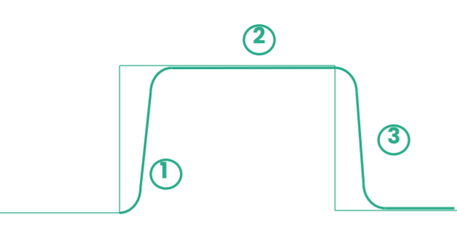
The advantage of using pressure sensor in mass flow controllers (MFC) is the response:
- With differential pressure measurement, the MFC can achieve the targeted mass flow much faster than thermal distribution measurement.
- In differential pressure MFC, PID control can be used during flow increase ①, steady state ②, and flow decrease ③.
- While in thermal distribution MFC, PID control can only be used during flow increase①.
Lithography machines are amongst the most critical machines in the semiconductor manufacturing process. In the laser control sub-system, Nitrogen gas control and protection against heat emanating from the laser beam is critical and must be supported with high accuracy pressure sensors.
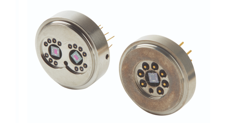
Druck's TERPS8100 is a highly accurate and stable pressure sensor used by lithography tool makers around the world to ensure production is not impacted by overheating. TERPS sensors are the most advanced sensor in our Industrial Sensor portfolio. They are offered across a wide selection of pressure ranges.
During the deposition process, known as chemical vapor deposition (CVD), a thin layer of dielectric or metallic film are deposited. These materials are key constituents of semiconductor devices.
Thermal processing in furnaces at temperatures up to 1200ºC, uniform film depositions or diffusion processes are achieved which are critical in the performance of any semiconductor device.
For both CVD and furnace processes the gas control by way of the MFC is critical in achieving the required deposition or diffusion.
Druck provides TERPS, ADROIT6200, and UNIK1000 pressure sensors to the industry, and they are widely recognized for their leading accuracy, long term stability and robustness. ADROIT6200 provides the accuracy needed for this application, and PACE5000 and 6000 pressure controllers are used for calibrating the MFC itself.
Precision is key in the dry etching processes for the semiconductor industry. Dry etch processes are used to precisely transfer the lithographically defined patterns of the integrated circuit into the surface of the wafer.
Druck solutions can be used in different ways during this process to help control pressure in the mass flow controller (MFC) and gas box systems to achieve very accurate gas flow control. Druck's PDCR1000 analog pressure modules and DPS5000 digital pressure sensors are core components in measuring absolute pressure and temperature to control helium gas flow rates. These products' stable outputs and fast responses to valve controls within the gas flow rate systems ensure pressure is optimized.
During this part of the process the wafer material is planarized to smooth surfaces through a combination of chemical and mechanical forces. An important controlling factor in the CMP process is the non-uniformity seen before and after polishing, which is theoretically dependent on a pressure distribution emanating from the polisher's downforce. The head of the polisher system needs to be calibrated and maintained in a way that produces fast and repeatable results for each wafer that passes through this process.
Our UNIK5000 configurable sensor coupled with Druck's Pressure Indicator and Loop Calibrator is ideal for constant control of pressure sensor applications to achieve consistent results during this process.
The most common lithography method is optical lithography, also known as photolithography. Photolithography is a fabrication process that patterns parts on thin film or wafer.
Deposition is a method where materials are deposited on a wafer surface as a thin layer.
Both wet and dry etching remove surface materials and create patterns on the surfaces. The main difference is that dry etching is done at the plasma phase and wet etching is done in the liquid phase.
Chemical mechanical polishing uses physical and chemical methods to surfaces of metal for semiconductor manufacturing.

