

スマートフォンやコンピューターから電気自動車や飛行機に至るまで、はんだ接合、半導体パッケージ、電気部品は、非常に重要なデバイスの多くにとって不可欠です。Waygate Technologies は、高解像度 2D X 線および 3D コンピューター断層撮影 (CT) 検査ソリューションを電子機器の生産ラインと研究開発ラボに提供し、コンポーネントの安全性と完全性を確実なものにします。

厳しい要件を満たし、製造とメンテナンスにおけるヒューマンファクターを減らす
パンデミックと原材料中心の市場 (バッテリー) の成長から、供給の安全確保が主要トレンドとなっています。
プリント回路板、コネクタ、家電などの製造およびテストで、高いレベルの精度と解像度が求められています。
個人のデバイスやウェアラブルデバイスを含め、すべてのセクターと産業の高まりで、電子機器と対応する原材料の需要が増加しています。
電子機器の供給と需要が増加していますが、そうした電子機器の再利用とリサイクルにはまだ問題が見られます... この循環経済でもっとやらなければならないことがあります。
当社は、電子機器産業向けのスマートかつ生産的で効率的な検査ソリューションを提供します
業界の課題に対応する技術
Li-ion batteries are among the most powerful energy storage devices commonly used in portable electronic devices, stationary power sources and electric vehicles. Our broad portfolio of premium radiography systems supports not only R&D as well as the post-mortem analysis of defective li-ion batteries to analyze the means of failure, but also fast CT inspection providing safe and secure production control with a reliable inspection of all vital parts.
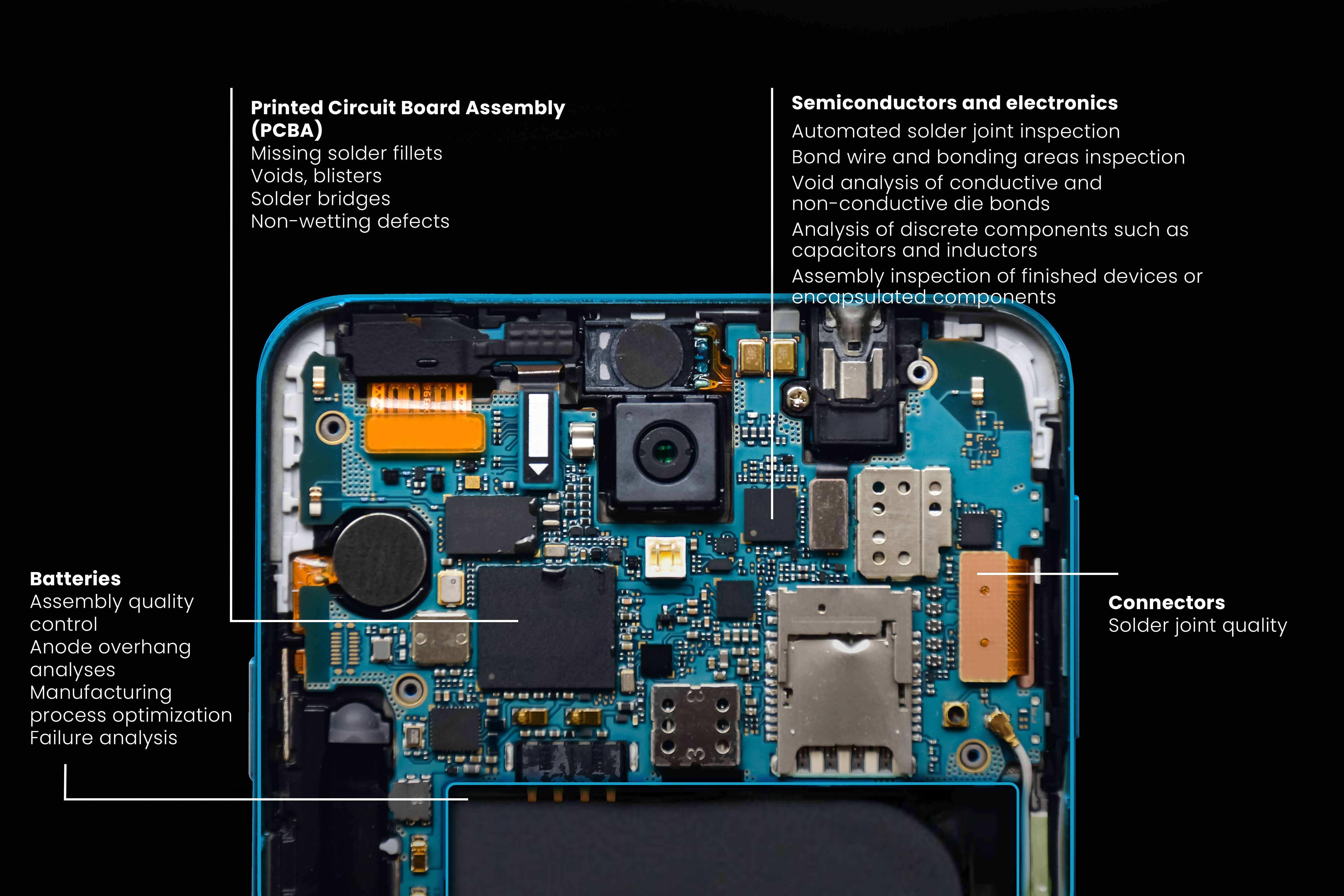
Because electronic components are becoming increasingly miniature and even more complex, high-resolution X-ray inspection has become a widely used tool for non-destructive failure analysis and process control in a variety of industrial and scientific fields. Our powerful nano- and microfocus X-ray technologies provide the means necessary to detect even the most minute defects in solder joints, bond wires and bonding areas, conductive and non-conductive die bonds, capacitors and inductors, finished assembly inspections, and more.
High-resolution X-ray technology is widely used in failure analysis and production quality testing of electronic devices to achieve more accurate inspections. Where standard 2D AXI does not allow reliable results due to overlaying features, our nano- and microfocus X-ray technologies provide clear slice views of packages or PCBSs. Any material flaw and quality characteristic affecting the shape of solder joints can be detected, like missing solder fillets, voids and blisters, solder bridges, or non-wetting defects.
