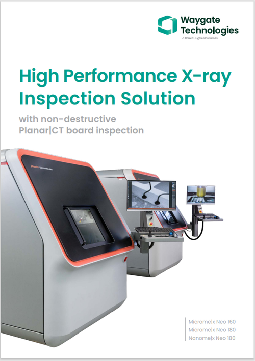

Premium Nanofocus and Microfocus Inspection for Electronics
The Phoenix Microme|x Neo and Nanome|x Neo provide high-resolution 2D X-ray technology, Planar|CT and 3D computed tomography (CT) scanning in one system.
With innovative engineering coupled with ultra-high positioning accuracy, Phoenix Microme|x Neo and Nanome|x Neo are ideally suited for industrial X-ray electronics inspections in process and quality control for greater productivity, failure analysis for the increased safety and quality of your products, and R&D where innovations are born. Both enable automated X-ray inspection (AXI) of electronic components - such as semiconductors, PCBs, electronic assemblies, sensors and lithium-ion batteries - in industrial, automotive, aviation and consumer electronics industries.
Non-destructive electronics inspection starts here
Innovative and unique features and an extreme high positioning accuracy make both the Phoenix MicromeIx 160 and 180 neo and the NanomeIx 180 neo the effective and reliable solution for a wide spectrum of 2D and 3D offline inspection tasks: R&D, failure analysis, process and quality control.
The Phoenix|x-ray X|act inspection software offers easy to program CAD based µAXI ensuring automated inspection in the micrometer range. Another unique benefit is Waygate Technologies’ rich options of DXR-HD digital detector fleet. There’s definitely a perfect match of image chain serving your particular application.
Product Highlights

- Large-size DXR S100 Pro detector in combination with superior pixel resolution defines industry leading imaging technology. Provides superior 100 µm pixel resolution and 30 cm x 25 cm large active area combining outstanding detectability with high inspection efficiency
- High dynamic DXR S140 detector with enhanced scintillator technology for precise and fast LIVE inspection. Full frame rate of 25 frames per second at 1536 x 1536 pixels offers low noise coupled with brilliant image quality ensuring fast and detailed live inspection

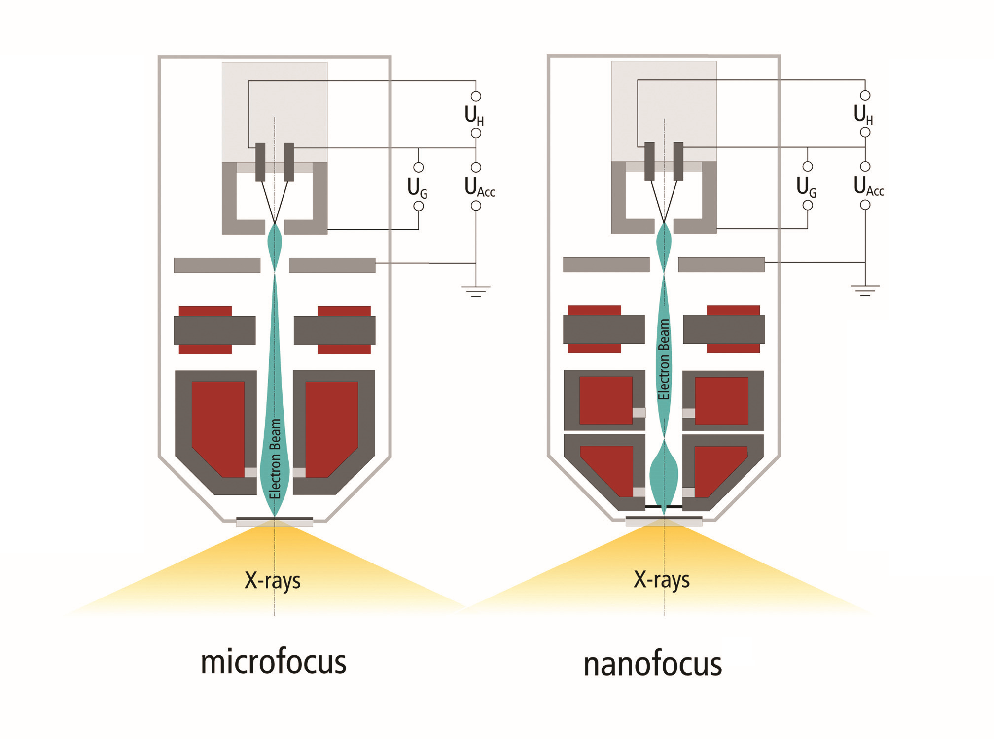
Compared to conventional beryllium targets, the Diamond|window allows higher power at a smaller focal spot. This ensures high-resolution
even at high output.
- Up to 2 times faster CT data acquisition at the same high image quality level
- High output with high-resolution
- Non-toxic target
- Improved focal spot position stability within long term measurements
- Increased target lifetime due to less degradation with higher power density

- Brilliant live inspection images with high dynamic Waygate Technologies DXR digital detector array
- Large 27” monitor and ultra-high defect coverage and repeatability
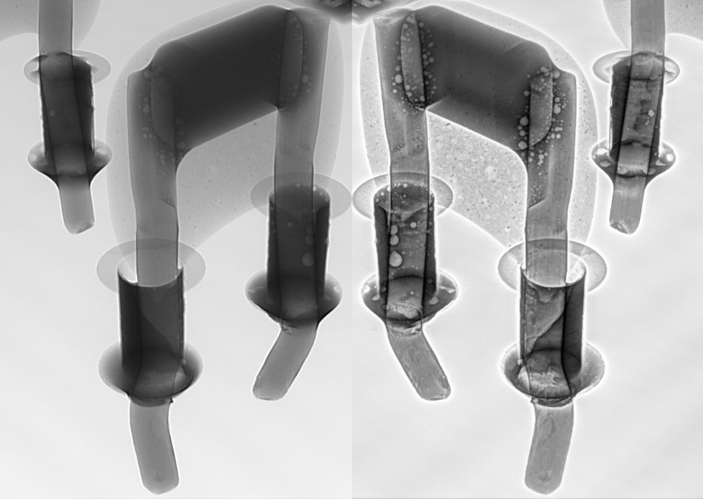
- Detail detectability at 0.5 µm or 0.2 µm with nanofocus
- Live overlay of CAD and inspection results even in rotated oblique inspection views
- High power 180 kV / 20 W microfocus or nanofocus tube for high absorbing electronic samples

Clear overview and fast positioning:
- Optical camera image or X-ray overview image for whole sample as navigation map
- Fast manipulation by clicking on the map
- Inspection program can be set based on the optical navigation map
- Position on the map can be saved into test report generated by X|act

- Shadow|target reduces unwanted radiation without frequent generator start & stop
- Fast and stable X-ray recovering. No delay of energy running up
- Realtime visualization of projected dose through “dose map” overlaid with Navigation map
- Cumulated dose calculation per inspection
- Multi-position dose measurement well integrated into inspection program
- Comparing with manual inspection, up to 99% radiation dose can be saved combining dose control technologies with automated inspection (programming)

X|act provides not only a minimal setup time compared to conventional view based AXI – once programmed, the inspection program is portable to all X|act compatible systems. The result is fast and easy programming: just assign the inspection strategies and let X|act generate the automated inspection program
- Specific inspection strategies for different pad types
- Fully automated inspection program generation
- Outstanding precision and repeatability - resolutions of only a few micrometers, 360° rotation, and oblique viewing up to 70°
- High reproducibility on large PCBs
- Easy pad identification by its live CAD data overlay function coupled with FLASH!™ image optimization
Benefits

Brilliant live inspection images due to high dynamic Waygate Technologies' DXR digital detector array
Unique high power 180 kV / 20 W micro- or nanofocus tube for even high absorbing electronic samples

Minimized setup time due to highly efficient automated CAD programming
Xe2 toolkit (X-ray image Evaluation Environment), a graphical based development environment for fast measure setups for evaluating X-ray images

Best detail detectability 0.5 μm or even 0.2 μm with nanofocus
Best in class image processing technologies optimize digital images quickly and constantly

Advanced failure analysis with high resolution 3D micro- or nanoCT® or large board Planar|CT
Optionally 3D CT scans less than 10 seconds
What Our Customers Are Saying
Technical Specification
Detail
Data
Spec
Phoenix Microme|x Neo 160
Phoenix Microme|x Neo 180
Phoenix Nanome|x Neo 180
Tube type
open microfocus
open microfocus
open nanofocus
Max. voltage / power
160 kV / 20 W
180 kV / 20 W
180 kV / 20 W
Max. detail detectability
0.5 µm
0.5 µm
0.2 µm
Resolution (Jima Structure)
2 µm
2 µm
0.8 µm
Max. inspection area
18” x 14”
24” x 20” w/o rotate table
18” x 14”
24” x 20” w/o rotate table
18” x 14”
24” x 20” w/o rotate table
Max. sample size
27” x 25”
27” x 25”
27” x 25”
Max. sample weight
10 kg / 22 lbs.
10 kg / 22 lbs.
10 kg / 22 lbs.
3D CT option
Yes
Yes
Yes
Plananr CT
Yes
Yes
Yes
Key application
PCB Inspection
PCB Inspection & Complex assembly
PCB Inspection & Complex assembly & Semiconductor
Microme|x Neo offers either a 160KV micro focus tube or a 180KV micro focus tube while Nanome|x Neo is equipped with a 180KV nano focus tube. The diamond window is installed as standard. Detail detectability at 0.5 µm (Microme|x Neo) or 0.2 µm (Nanome|x Neo). 20W power on target for all tube fleet contributes to high inspection resolution and throughput.
Microme|x Neo and Nanome|x Neo offer various detectors with unique features fulfilling your particular application,
- 75 µm resolution DXR S85 detector of price-performance ratio for small components and PCB/PCBA inspection
- 200 µm resolution DXR 250RT with active cooling of extremely high dynamic range and brilliant image quality ensuring fast and detailed live inspection
- 139 µm resolution DXR S140 with super fast imaging meeting comprehensive needs of high integrated micro electronics inspection
- 100 µm resolution large size DXR S100 Pro detector offering outstanding combination of detectability and productivity, perfectly fitting semiconductor and large sample inspection
The Max. inspection area of our system is 460 mm x 360 mm (18” x 14”) with a rotation table, and 610 mm x 510 mm (24” x 20”) with an optional X-Y table (non-rotatable). Max. sample size/weight is 680 mm x 635 mm (27” x 25”) / 10 kg (22 lbs.).
Microme|x Neo and Nanome|x Neo is equipped with high-precision 5-axis manipulator platforms - X, Y, Z, tilt and rotate axis.
Open tube technology provides an X-ray tube with unlimited lifetime. The tube can be quickly restored to optimal performance by replacing the filament. The plug-in cathode used by Microme|x Neo and Nanome|x Neo has an integrated filament, which allows customers to replace it quickly and easily, minimizing system down time.
Phoenix|x-ray’s proprietary 3D CT technology is optionally available on the Microme|x Neo and Nanome|x Neo for advanced inspection and 3D analysis of smaller samples. Max. geometric magnification could be 100x (CT) and Max. voxel resolution down to 2um, resolution depending on the sample size.
Easyfix|CT, 3D cone beam CT, can deal with all the small samples. When the sample is too large to be rotated, Planar|CT can be used for 3D imaging avoiding sample cutting.
You need nothing more than one click!
Combining 25+ years of experience and patents with next-generation technology, Waygate Technologies’s intelligent Flash!™ software automatically optimizes your digital radiographs quickly and consistently. The balanced presentation of different densities and materials lets you see all the subtle details in one single image, with no manual adjustments.
And now the newest version specially optimized for electronics, Flash! Electronics, is available!
Some radiation sensitive electronics such as memory and resistor will get damaged by certain dose. Therefore, the radiation dose needs to be strictly monitored and managed for reducing the quality (inspection) cost as much as possible. Waygate Technologies’ low dose management bundle is a comprehensive solution which combines Shadow|target and Dose|manager enabling dose control from both X-ray source and receptor end.
Dose control is well integrated with inspection programming and fitting various applications.
Absolutely yes. The X|act software on the Microme|x Neo and Nanome|x Neo provides various levels of automated inspection procedures
View based and CAD based programmable and intelligent process with automated image processing.
Wizard guided solder joint modules for easy setup of e.g. voiding calculation or BGA inspection tasks.
Image processing toolkit “Xe²”, extremely powerful evaluate tool that can be programmed by users with human logic language and adapted for the X-ray inspection process of various application.
OPC-UA based software communication protocol to enable integration with automation subsystems such as sample loader (not standard in X|act)
Microme|x Neo and Nanome|x Neo uses proprietary OVHM technology to achieve tilt view. And they are the only systems on the market that places the tube above the sample and the FPD below the sample. The unique benefit is:
Operator sees the sample exactly as it appears in the X-ray image (intuitive inspection)
Tube can be as close as possible to the sample to achieve highest magnification.
Precision manipulator locks field of view during rotation and OVHM tilt
Phoenix Microme|x and Nanome|x Industrial Radiography Solutions


Resources